NorthEast RF, 531 Stuyvesant Ave, Union County, New Jersey 07083
Antenna Matching
Antenna Impedance Matching
Antenna impedance matching is the process of reducing the conducted power losses between the antenna and active electronics; and good transmission line design provides low loss conducted RF signal paths. This can help overcome link reliability and improve device operating range.

Multi-band antennas can be particularly challenging. For example, the 5GHz WiFi ac band is very sensitive to component layout and parasitic effects. Particularly difficult are cellular LTE-M and NB-IOT low band antenna matching, where the antenna location and length of PCB have a profound effect on return-loss and efficiency necessary to meet carrier compliance.
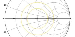
The matching circuit performance is typically characterized using return loss. To obtain an efficient and robust network requires that component losses, tolerances, PCB materials, and topology are considered. NorthEast RF antenna matching service starts at $2880 for a basic antenna or $4800 for a multi-band antenna such as dual-band WiFi or LTE. See our price list here.
Workflow - Impedance Matching
Depending on the project development phase you supply two PCBs or devices (with enclosure) – It’s easy to damage tracks so we like a spare. Schematic diagram and BOM.
A coaxial cable is soldered to the antenna matching circuit. Using a vector network analyzer (VNA), the cable losses and phase length are calibrated at the antenna interface and the return loss measured. Next the DUT is then connected to the antenna test system to measure the antenna efficiency along peak gain and radiation pattern. This provides a baseline of the device performance before modification.
To simulate a new matching topology, firstly the old matching network is removed. A coaxial connection re-located to the base of the antenna feed. S-parameters are measured and transferred to a matching tool. Next, a robust matching circuit is synthesized that will provide the required return loss over the operating band after taking component tolerances into account. Several iterations of the matching network are often required, particularly with multi-band antennas such as LTE.
The theoretical matching network component values are added to the antenna one component at a time. Each component is adjusted to achieve the correct impedance at the given node. Sometimes the component locations are not suitable regardless of what the antenna manufacturer has stated in their data sheet. This is generally due to the location of antenna, size and shape of PCB. All of these factors affect the required matching topology.
To confirm the end of design cycle, the antenna efficiency is measured and compared against the baseline measurements. Depending on the performance achieved, we either move to final report or discuss our findings with the client.
The project is completed with a report. This comprises the performance, matching circuit topology and BOM.
Transmission Line Design

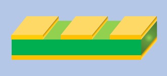
It is easy to end up with a lossy printed RF signal trace between antenna and active device. This is usually due to either the layer stack dimensions, PCB material, or ratio of trace width to substrate height. Even via hole locations can have an impact on the characteristic impedance. Our Transmission line design workflow covers all these details and will result in a low loss connection between the active device and antenna matching circuit.
Workflow - Transmission Line
You supply GERBER files, layer stack, circuit diagram and aPCB with existing transmission line if available.
If a PCB is available, we will measure the transmission line characteristic impedance and insertion loss. A coaxial cable is soldered to either end of the transmission line. Then a vector network analyzer is connected and the cable losses and electrical length are calibrated. The insertion loss is then measured to determine if its performance is commensurate with simulated performance.
We use a transmission line calculator along with our knowledge of suitable materials and width to height ratios to achieve a well defined RF trace that provides the required characteristics. Likely this will require minor changes to your layer stack and material selection. Therefore, we liaise with PCB layout and design engineer to establish a suitable compromise.
If a standard microstrip | CPW | stripline is not feasible, then we will use a field simulator to determine the transmission line geometry.
The project is completed with a report. This comprises a revised layer stack, material selection and transmission line geometry.